Wafer Bonder/Debonder Synapse™ Series
Support mass production of 3D integration with reliable technology

Synapse™ series became an industry standard Bonding/DeBonding tools for 300mm wafers, by combining TEL’s leading-edge technologies such as ultra-thin wafer transfer, chemical coating, plasma processing and cleaning developed over the 50 years of history. Synapse™ series provide advanced solutions for temporary Bonding/DeBonding process in TSV (Through Silicon Via), permanent bonding process for CMOS image sensor and other various types of devices to contribute to high volume manufacturing of 3D integration which becomes even more important and expected to grow.
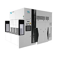
Synapse™ Si is a successor model of Synapse™ S, a wafer fusion bonding equipment widely used in 300mm CMOS image sensor mass production lines. Compared to conventional Synapse™ S, alignment accuracy has been improved. In addition, Synapse™ Si adopts a compact design that halves the footprint, and also realized high throughput at the same time. By extending additional block, productivity per footprint can be further improved. Highly reliable LITHIUS Pro™ Z platform is adopted and realize high user interface. By following the design of cleaning modules and plasma processing modules that have been proven in front-end process, it achieved high mass production reliability as a 300 mm wafer bonding system. Not only as bonding of silicon oxide film wafers but also as Cu hybrid bonding for mass production line. Deployment to various applications besides CMOS image sensors is expected in the future. TEL will contribute to the development and mass production of these new applications.
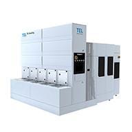
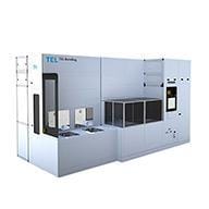
Synapse™ V and Synapse™ Z Plus, these systems are 300mm wafer bonder/debonder system which enable temporary bonding or debonding process efficiently. As the continuation of Moore’s law is becoming more and more challenging, 3D-IC with through-silicon via (TSV) interconnects secure a firm position in the field of advanced semiconductor, attracting attention as a means to improve semiconductor performance. Synapse™ V is a temporary wafer bonding system, which allows two wafers to be bonded together by using various adhesives. The system consists of material coating, baking, and bonding functions to realize integrated wafer bonding processes in a single tool. Uniquely developed wafer alignment unit and wafer bonding module provide the highest level of Total Thickness Variation (TTV) and bonding accuracy. Synapse™ Z Plus, equipped with wafer debonding, device and carrier wafer cleaning function, makes it possible to complete complicated wafer debonding process after TSV process with one system. The system has newly developed special function that provides stabilize transfer and safe process operation of ultra-thin wafers less than about 50um thickness.
Product comparison
 |
 |
 |
|
| Wafer size (mm) |
300 | 300 | 300 |
| Availability | New | New | New |
| Typical Applications | BSI | TSV | TSV |
| Accuracy | 3σ<100nm (Alignment accuracy) |
<5% (TTV of glue thickness) |
ー |
| Additional features | High-alignment accuracy, High-reliability |
Up to 3layer of glue | Mechanical-Debonding, Carrier wafer cleaning capability |
Synapse is registered trademark or trademark of Tokyo Electron Group in Japan and/or other countries.


