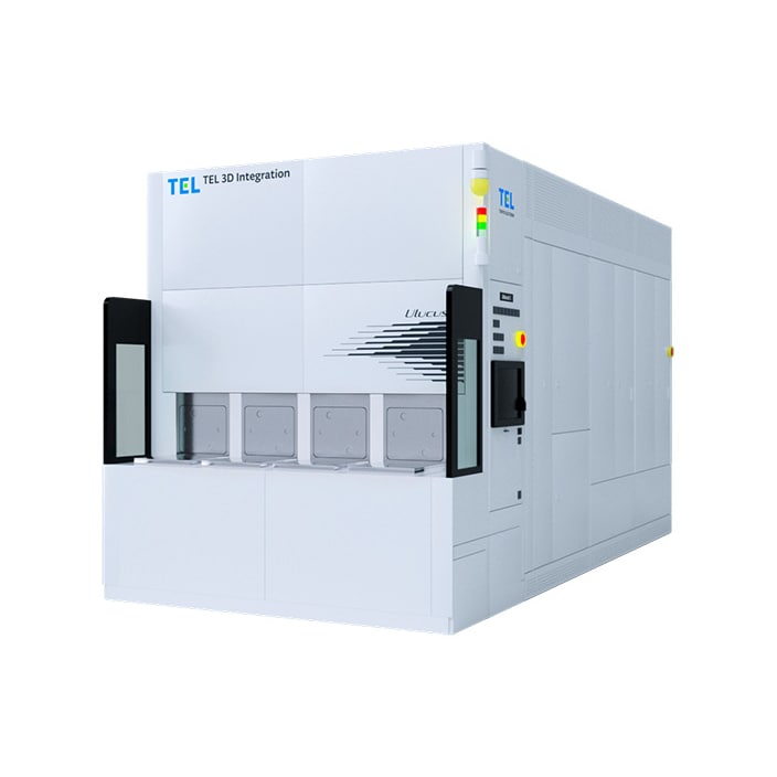
Wafer Edge Trimming Ulucus™ L Series
TEL’s technology drives innovation in 3D high-density packaging processes

The Ulucus™ L series of semiconductor production equipment integrates TEL’s market-leading and production-proven Coater/Developer platform technology with several advanced technologies including wafer cleaning. As further semiconductor scaling and performance enhancements are crucial to such devices as CMOS image sensors, next-generation memories, and advanced logic chips, chip manufacturers are increasingly adopting 3D high-density packaging technologies using permanent wafer bonding methods. TEL anticipates a significant growth in permanent wafer bonding processes, and has introduced high-volume processing systems equipped with innovative technologies to address the customers’ production needs.
Ulucus™ L is a laser edge trimming system for 3D high-density packaging of 300mm devices. The system integrates TEL’s production-proven Coater/Developer platform technology with an advanced and highly original laser controller unit, enabling super clean technology comparable to that available in front-end processes in addition to excellent reliability and productivity. The system uses laser control technology to produce high-quality cut surfaces through precise and speedy edge trimming operations. The use of a dry laser process that does not require deionized water (DIW) ensures reduction in DIW consumption, dust emissions, and wastewater discharges. Since edge trimming is performed after the wafer bonding, fewer process steps are required before and after trimming.
Ulucus is a registered trademark or trademark of Tokyo Electron Group in Japan and/or other countries.

